
IBM has announced plans to build a $2 billion quantum chip foundry in Albany, New York, with half the funding coming from the US government. The Trump administration has awarded IBM $1 billion as part of a broader push to establish domestic leadership in quantum computing. IBM will match this investment, and together they will form a new company called Anderon, which will operate the first purpose-built quantum chip fabrication unit in the United States.
A Quantum Leap for US Manufacturing
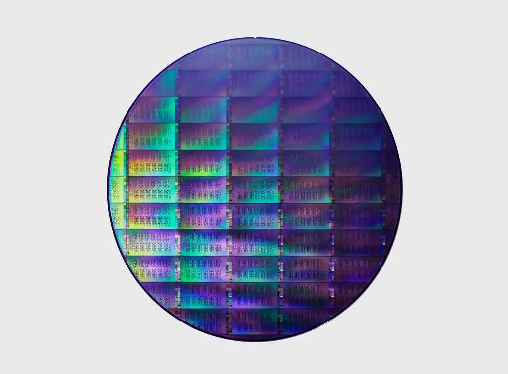
Quantum computing represents a paradigm shift from classical computing, leveraging the principles of quantum mechanics to solve problems that are currently intractable. Central to this technology is the quantum chip, which requires fabrication processes vastly different from traditional silicon semiconductors. Quantum bits, or qubits, must be isolated from environmental noise to maintain coherence, demanding ultra-pure materials and extreme precision in manufacturing.
IBM has been at the forefront of quantum research for decades, investing heavily in both hardware and software. The company's recent advancements include the IBM Osprey processor with 433 qubits and the roadmap toward a 1,121-qubit Condor chip. However, scaling up production has remained a bottleneck, which the new foundry aims to address.
“Our work in silicon wafer fabrication has been a key to IBM’s success and will be critical to enable a broader quantum technology landscape,” said IBM CEO Arvind Krishna. “Anderon will be well-positioned to fuel America’s fast-growing quantum technology industry.” The new facility will leverage IBM's expertise in semiconductor manufacturing while adapting processes to the unique demands of quantum chips.
Anderon: A Dedicated Quantum Foundry
Anderon will not exclusively serve IBM; it will develop quantum wafers for a variety of hardware vendors. This open approach is intended to accelerate the entire quantum ecosystem by providing a shared, state-of-the-art manufacturing resource. Unlike classical chip foundries that churn out millions of identical processors, quantum foundries must handle a diverse range of qubit technologies — superconducting circuits, trapped ions, photonic qubits, and more. Anderon aims to be flexible enough to support multiple architectures, thereby reducing entry barriers for smaller quantum startups.
The choice of Albany, New York, is strategic. The region already hosts the SUNY Polytechnic Institute's Colleges of Nanoscale Science and Engineering, which has a deep talent pool in nanotechnology and semiconductor fabrication. New York State has also been aggressive in attracting high-tech manufacturing, offering tax incentives and infrastructure support. IBM's existing facilities in the area include research labs and development centers, making Albany a natural hub for this quantum initiative.
Construction of the foundry is expected to begin later this year, with initial production lines operational by 2028. IBM estimates that the facility will create over 1,000 direct jobs and thousands more in the supply chain. The company also plans to partner with local universities to train the next generation of quantum chip engineers.
Government Investment in Quantum Technology
The US government's $1 billion grant is part of a larger quantum technology investment strategy. The administration also awarded funds to GlobalFoundries, D-Wave Quantum, and Rigetti Computing, signaling a comprehensive effort to secure American leadership in this critical field. GlobalFoundries will focus on manufacturing classical chips optimized for quantum control electronics, while D-Wave and Rigetti will advance their respective quantum annealing and gate-model systems.
This public-private partnership mirrors similar initiatives in Europe and Asia, where governments are racing to build quantum infrastructure. China, for example, has invested billions in a national quantum laboratory and has already demonstrated quantum supremacy with its Zuchongzhi processor. The US response aims to ensure that the next generation of quantum computers — those capable of solving real-world problems in cryptography, drug discovery, materials science, and climate modeling — are developed and manufactured domestically.
Quantum Computing: The Bigger Picture
Quantum computing is still in its infancy, but the potential rewards are enormous. Google, Microsoft, Intel, and a host of startups are all chasing the same goal: a fault-tolerant quantum computer with millions of qubits. IBM's approach has been to gradually scale up superconducting qubits while developing error mitigation techniques that allow practical computations on current noisy devices. The IBM Quantum Network already connects over 200 organizations worldwide, offering cloud access to quantum processors.
The establishment of a dedicated quantum foundry is a recognition that manufacturing is as important as design. Just as the semiconductor industry relies on foundries like TSMC and Samsung to produce advanced chips, quantum computing will need specialized fabrication facilities. Anderon's model could become the blueprint for a future quantum manufacturing sector.
Maxwell Cooter, the journalist who broke this story, noted that the announcement has been met with excitement in the quantum community. “This is a game-changer,” said Dr. Sarah Jennings, a quantum physics professor at MIT. “Having a purpose-built foundry means we can iterate faster on qubit designs, move beyond lab-scale prototypes, and start producing chips that are reliable and reproducible.”
The foundry will also address the growing demand for quantum components in adjacent fields. Quantum sensors, quantum communication devices, and quantum random number generators all require similar fabrication techniques. Anderon could become a one-stop shop for many of these technologies, further cementing New York's status as a quantum technology center.
IBM's timeline for the foundry includes a pilot phase where processes are validated, followed by a ramp-up to commercial production. The company expects to serve not only its own quantum processors but also those of partners who lack in-house fabrication capabilities. This open foundry model could democratize quantum hardware development, allowing startups to focus on architecture and algorithms without the massive capital expenditure of building a factory.
While $2 billion is a substantial investment, it pales in comparison to the cost of classical semiconductor fabs, which can exceed $10 billion. Quantum foundries are less capital-intensive because they require smaller wafer volumes and less complex lithography. However, the precision required is far greater, and the need for cryogenic testing adds complexity. Anderon plans to incorporate advanced automation and AI-driven process control to maintain high yields.
Implications for the Quantum Ecosystem
The Anderon announcement is likely to spur similar initiatives in other countries. The European Union has already launched the Quantum Flagship program, and the UK is building a National Quantum Computing Centre. Japan and South Korea are also investing in quantum infrastructure. The competition is fierce, but the US now has a clear advantage with a dedicated manufacturing facility.
For IBM, this move reinforces its commitment to quantum technology as a core business. The company has already commercialized quantum services through IBM Quantum, and the foundry will ensure a steady supply of chips as demand grows. Most immediately, Anderon will help IBM meet the needs of its existing partners in finance, logistics, and energy, many of whom are exploring quantum applications.
One potential bottleneck is the supply of raw materials. Superconducting qubits typically use niobium or aluminum, both of which are widely available. However, some advanced qubit designs require exotic materials like tantalum or indium arsenide. IBM is likely to work with suppliers to secure a stable supply chain, possibly through long-term agreements.
The success of Anderon will depend on its ability to attract customers from a diverse quantum landscape. Companies like IonQ (trapped ions), PsiQuantum (photonic qubits), and Quantinuum (trapped ions) each have unique fabrication requirements. Anderon must develop a flexible process flow that can accommodate different qubit technologies without compromising performance. This is a significant technical challenge, but IBM's decades of experience in semiconductor innovation provide a strong foundation.
Finally, the foundry will serve as a training ground for the quantum workforce. Partnerships with Albany's universities will create internships and apprenticeship programs, ensuring that the next generation of engineers is ready to work in quantum manufacturing. This educational component is vital for sustaining long-term growth in the industry.
Source: Network World News